

Homray Material Technology(HMT)was established in 2009, is a leading manufacturer and supplier of Gallium Nitride(GaN) Wafer, GaN Substrate Wafer, Silicon Carbide(SiC) Wafer, SiC Substrate Wafer, 4H-N/4H-SI SiC Substrate, and GaN Epi Wafer (GaN-On-Si, GaN-On-Sapphire, GaN-On-SiC ), SiC Epi Wafer etc. It is widely acknowledged that compound Semiconductor (GaN, SiC) with its superior property like wide-bandgap, is expected to the most promising material choice for next generation device. GaN device/module and SiC device/module can achieve low losses and fast switching/oscillation simultaneously because of its high critical electrical field. Homray Material Technology is committed to developing high quality GaN Wafer and SiC Wafer for HEMT RF, power electronics and opto-electronics applications. As the leading Substrate Wafer and Epi Wafer manufacturer and supplier in the semiconductor industry, our dealers and partners are mainly
4 Inch GaN-On-Sapphire Template Manufacturer
Dimensions: Ф 100 mm ± 0.1 mm
Thickness:4.5 µm, 20 µm
Orientation:C-plane(0001) ± 0.5°
Useable Surface Area:> 90%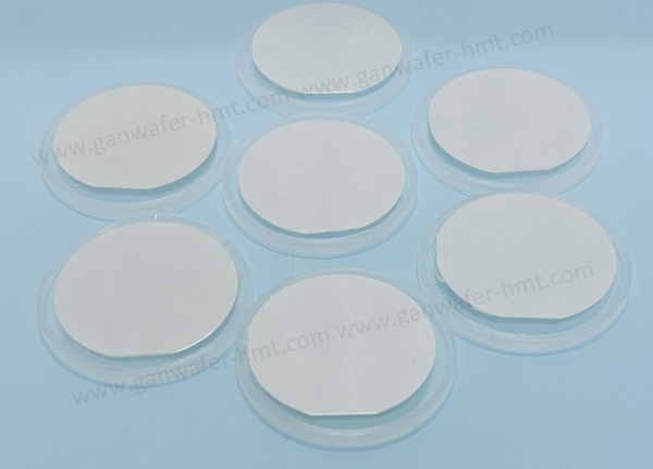
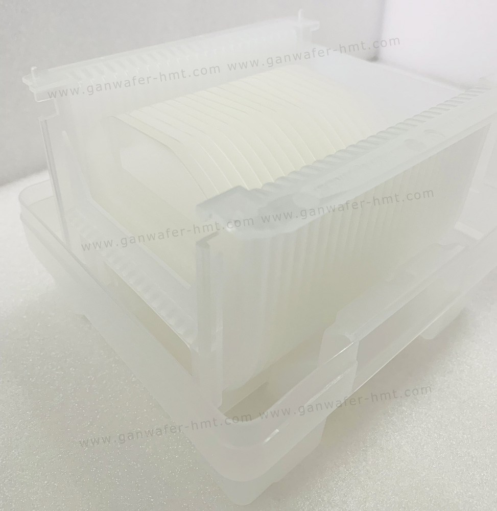
2 Inch Free-Standing GaN Substrate Supplier
Dimensions: Ф 50.8 mm ± 1 mm
Thickness: 350 ± 25 µm
Useable Surface Area: > 90%
Total Thickness Variation: ≤ 15 µm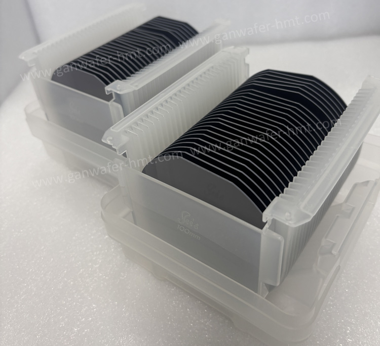
4 inch D-HEMT GaN On Si Epi Wafer Supplier
GaN-On-Si Epi Wafer For Power HEMT D-Mode
Substrate Diameter: 2inch,4inch,6inch, 8inch
Substrate Thickness: 675,1000um
Epi Layer Total Thickness: 2~5.5um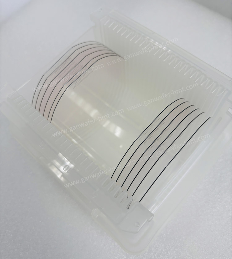
4 inch 6 inch GaN On SiC Epi Wafer Manufacturer
GaN-On-SiC Epi Wafer For RF HEMT
Substrate Size: 2''3''4''6''
Substrate Thickness: 350um 500um
GaN Buffer Layer: 1.8um
AIN Spacer: 1nm
![]() M.P: +86-15366208370 ; +86-15366203573
M.P: +86-15366208370 ; +86-15366203573
![]() E-mail: kim@homray-material.com tina@homray-material.com
E-mail: kim@homray-material.com tina@homray-material.com
HMT Silicon Carbide (SiC) Substrate Website: www.sicsubstrate-hmt.com