
D-HEMT/E-HEMT GaN on Si Epitaxial Wafer
Project Description
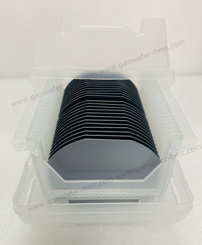
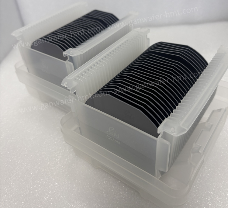
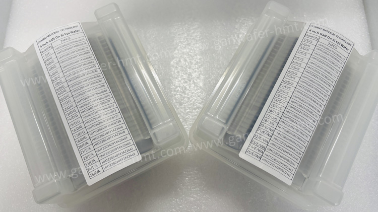
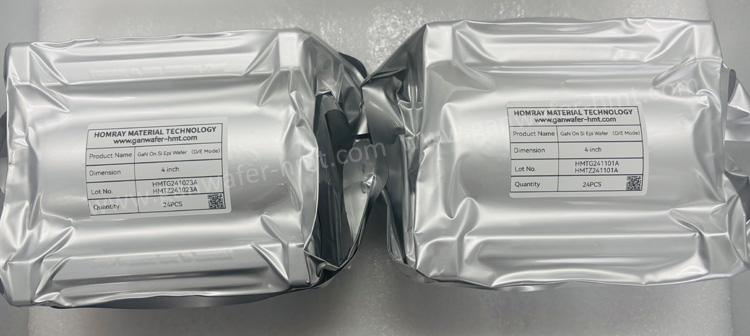
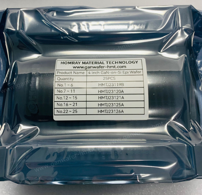
HMT provides GaN Epi wafer solutions for advanced semiconductor applications. We deliver high-quality GaN-on-Si wafers in 4-inch, 6-inch, and 8-inch diameters, supporting D-Mode, E-Mode, and RF structures. Our specialized epitaxial growth expertise, honed over years of collaboration with global leaders, ensures unmatched performance and reliability for your Power HEMT and RF devices. Let's collaborate to define the future of power electronics.
![]() E-mail: kim@homray-material.com tina@homray-material.com
E-mail: kim@homray-material.com tina@homray-material.com
HMT Silicon Carbide (SiC) Substrate Website: www.sicsubstrate-hmt.com