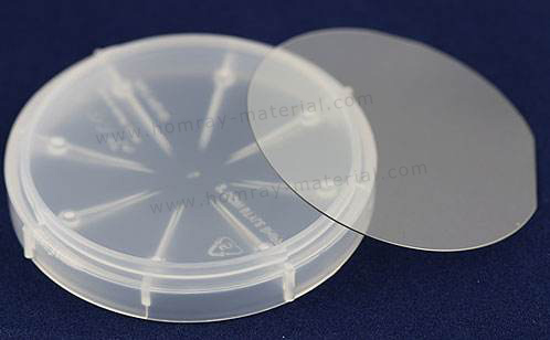
Homray Material Offers Gallium Nitride Wafer/GaN Substrate
Homray Material Technology is specialized in providing silicon wafer/Epi wafer , silicon carbide wafer/Epi wafer , sapphire wafer,GaN wafer( gallium nitride wafer)and various consumables for silicon wafer, silicon carbide wafer, sapphire wafer slicing, polishing and lapping machine.
 We are pleased to offer GaN substrate to our customers including many who are developing better and more reliable for GaN HEMTs, which have found immediate use in various wireless infrastructure applications due to their high efficiency and high voltage operation. Second generation technology with shorter gate lengths will be addressing higher frequency telecom and aerospace applications. Our GaN substrate has excellent properties, it’s a very hard, mechanically stable wide bandgap semiconductor material with high heat capacity and thermal conductivity. In its pure form it resists cracking and can be deposited in thin film on sapphire or silicon carbide, despite the mismatch in their lattice constants. GaN can be doped with silicon (Si) or with oxygen to n-type and with magnesium (Mg) to p-type; however, the Si and Mg atoms change the way the GaN crystals grow, introducing tensile stresses and making them brittle. Gallium nitride compounds also tend to have a high dislocation density, on the order of a hundred million to ten billion defects per square centimeter. The availability improve boule growth and wafering processes." and "Our customers can now benefit from the increased device yield expected when developing advanced transistors on a square substrate. Our GaN substrate are natural by products of our ongoing efforts, currently we are devoted to continuously develop more reliable products.
Gallium nitride (GaN) is a binary III/V direct bandgap semiconductor commonly used in light-emitting diodes since the 1990s. The compound is a very hard material that has a Wurtzite crystal structure. Its wide band gap of 3.4 eV affords it special properties for applications in optoelectronic, high-power and high-frequency devices. For example, GaN is the substrate which makes violet (405 nm) laser diodes possible, without use of nonlinear optical frequency-doubling.
Its sensitivity to ionizing radiation is low (like other group III nitrides), making it a suitable material for solar cell arrays for satellites. Military and space applications could also benefit as devices have shown stability in radiation environments.Because GaN transistors can operate at much higher temperatures and work at much higher voltages than gallium arsenide (GaAs) transistors, they make ideal power amplifiers at microwave frequencies. In addition, GaN offers promising characteristics for THz devices.
For more information, please visit our website: http://www.homray-material.com,or send us email kim@homray-material.com/tina@homray-material.com.