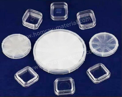
 With the development of silicon-based technology gradually approaching the limit, Silicon Carbide (SiC), Gallium Nitride (GaN) presented by the third generation of semiconductors ushered in the explosion. Among them, SiC and GaN as the most mature, the highest degree of commercialization of the third generation of semiconductor materials are natural limelight.
As the leading manufacturer of free-standing GaN wafer, HMT provide 2 inch and 4 inch GaN template (GaN Epi on Sapphire substrate). We also offer cutomzied GaN Epitaxial wafer for LED application with blue light and green light. Please contact us and let us know your detailed requirement.
Gallium nitride(GaN) is mainly synthesized as a semiconductor material with a band gap of more than 2.3eV, also known as a wide band gap semiconductor material, which is a new material for developing microelectronic devices and optoelectronic devices. Compared with "Get Silicon Carbide Gets The World", GaN Material is much lower profile. In 1969, Japanese scientist Maruska and others deposited GaN film on the surface of sapphire substrate, GaN entered the rapid development stage at the beginning of this century. Gallium nitride first entered mainstream consumer application in 2019 as one of the main materials for third-generation semiconductors, and gained attention in 2020 with xiaomi Gallium Nitride Charger.
As the third generation of semiconductor materials, GaN is often compared with silicon carbide(SiC). Although GaN has not developed for a long time as silicon carbide, it still shows its advantages by virtue of its large band gap, high breakdown voltage, high thermal conductivity, high saturated electron drift speed and strong radiation resistance. According to the GaN Power 2021 report published by Yole Developpement, the GaN Power market is expected to reach $1.1 billion by 2026.