
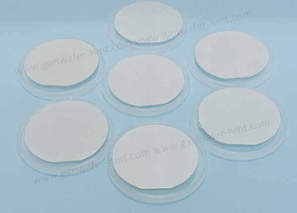
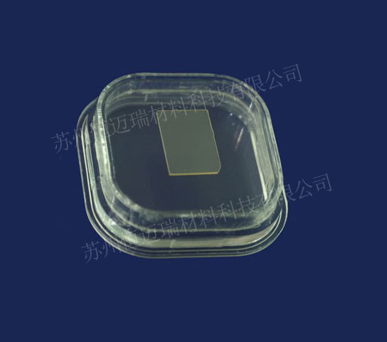
4 Inch Free-Standing Pure GaN Wafer Manufacturer
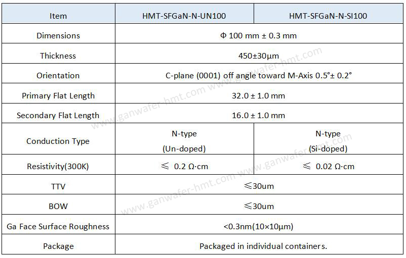
Dimensions: Ф 100 mm ±0.3mm
Thickness: 400 ± 50 µm
Useable Surface Area: > 90%
Total Thickness Variation: ≤ 30 µm
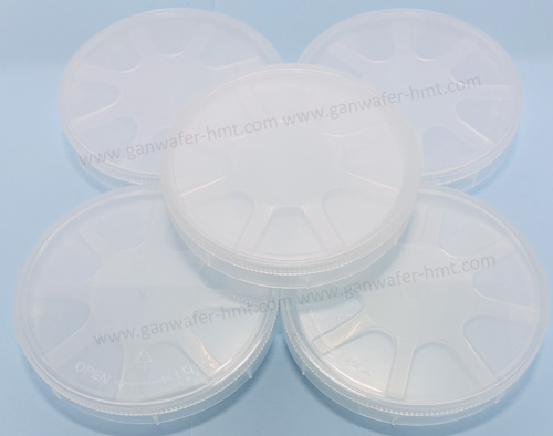
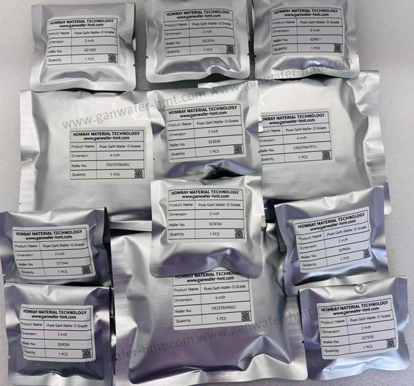
Product Description
As the Global manufacturer of Free-standing GaN Substrate Wafer, Homray Material Technology can provide 4 inch N type Free-Standing GaN Substrate wafer including un-doped and Si-doped N type. The thickness of GaN substrate wafer is 450um. GaN based systems have higher power efficiency, thus reducing power losses, switch at higher frequency, thus reducing size and weight.
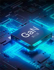
GaN technology is used in numerous high-power applications such as industrial, consumer and server power supplies, solar, AC drive and UPS inverters, and hybrid and electric cars. Furthermore, GaN is ideally suited for RF applications such as cellular base stations, radars and cable TV infrastructure in the networking, aerospace and defense sectors.
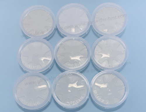
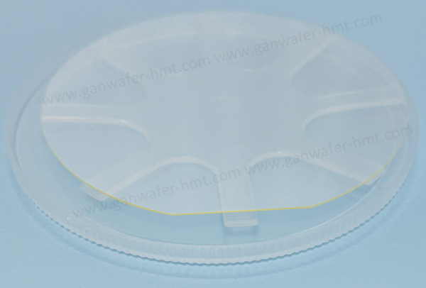
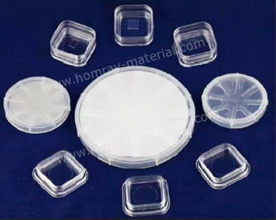
Related Products
![]() E-mail: kim@homray-material.com tina@homray-material.com
E-mail: kim@homray-material.com tina@homray-material.com
HMT Silicon Carbide (SiC) Substrate Website: www.sicsubstrate-hmt.com