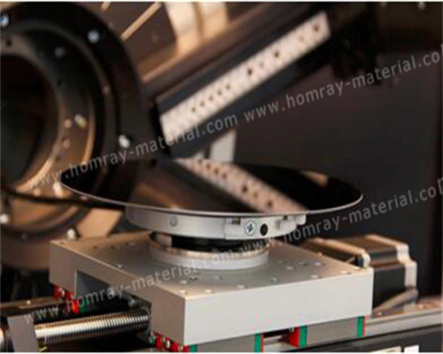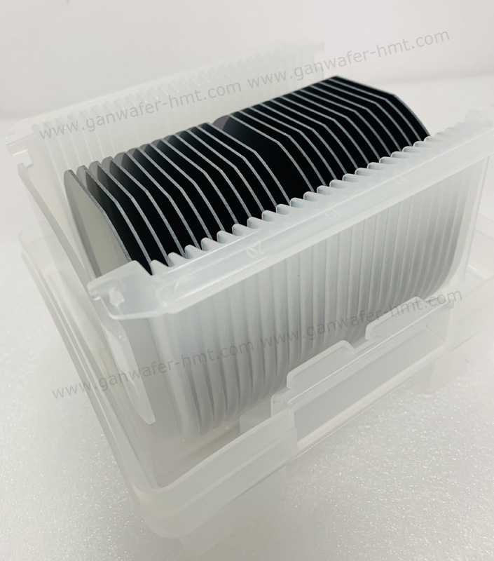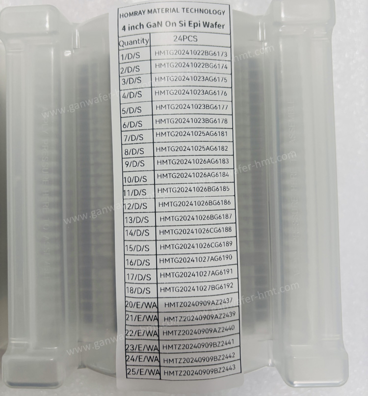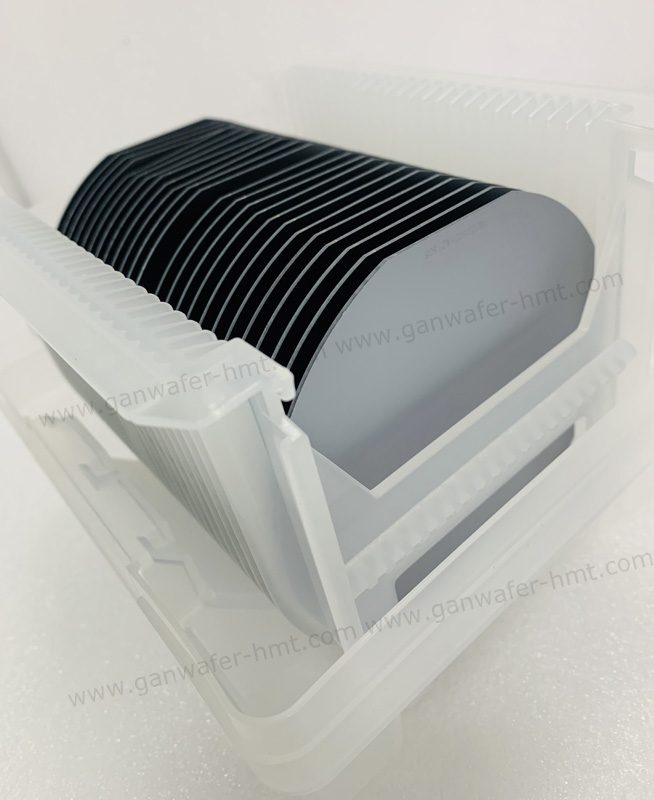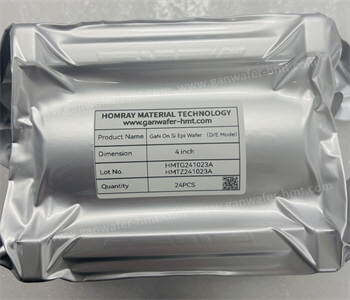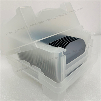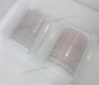
4 inch D-HEMT GaN On Si Epi Wafer Supplier
GaN-On-Si Epi Wafer For Power HEMT D-Mode
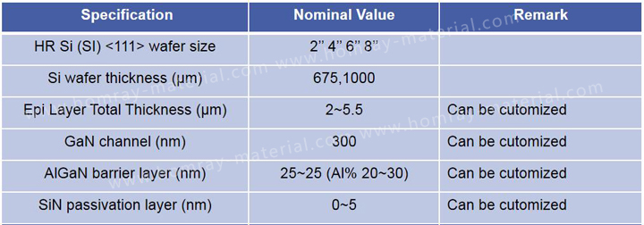
Substrate Diameter: 2inch,4inch,6inch, 8inch
Substrate Thickness: 675,1000um
Epi Layer Total Thickness: 2~5.5um
Product Description
HMT is a trusted manufacturer of GaN-On-Si Epi Wafer For Power HEMT application. Homray Material Technology mainly offers 100mm4inch and 150mm6inch GaN-on-Si Epi wafer for power switching. The HMT650V product is a state-of-the-art (Al,Ga)N/GaN heteroepitaxial layer structure deposited crack-free on a (111) Si-wafer for high voltage power switching applications. We can offer the best prices on the market for high quality GaN Epi wafers. Customers from all over the world have trusted HMT as their preferred supplier of GaN epi-wafers and GaN transistors.
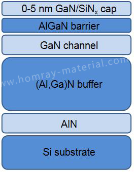
The epitaxial layer consists of an active heterostructure based on an AlGaN layer and a GaN channel, providing high electron mobility and low sheet resistivity.The proprietary high-voltage buffer design offers low leakage currents, high breakdown voltage, low dispersion and a consistently low wafer bow.
Standard Layer Specifications For Power HEMT-D mode
Standard Layer Structure Key Features
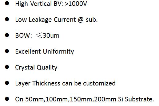
Characterization Specifications

Related Products

