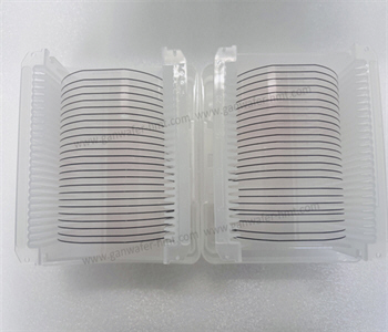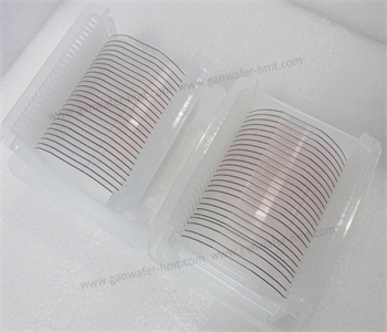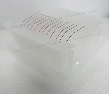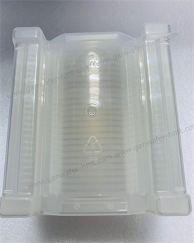
AlGaN/GaN On SiC HEMT Epi Wafer Manufacturer
Spec: 4 inch or 6 inch
Substrate: 4H-SiC
Thickness: 500um
Type: Semi-insulating
Product Description
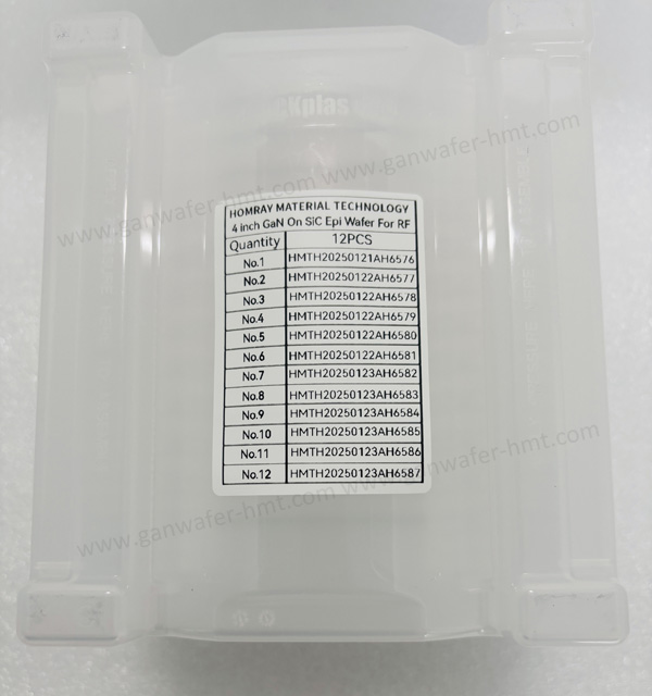
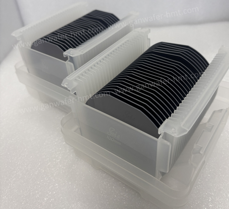
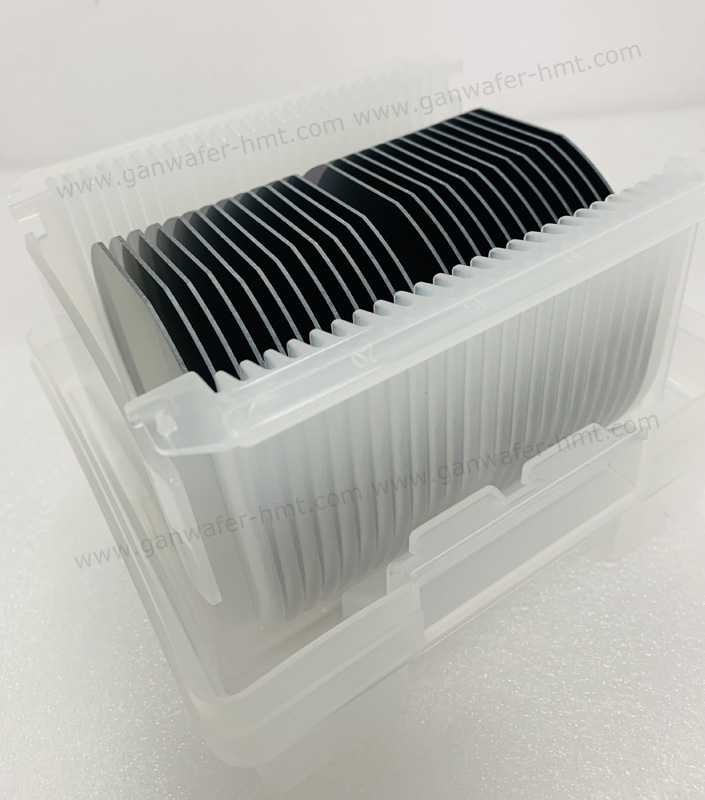
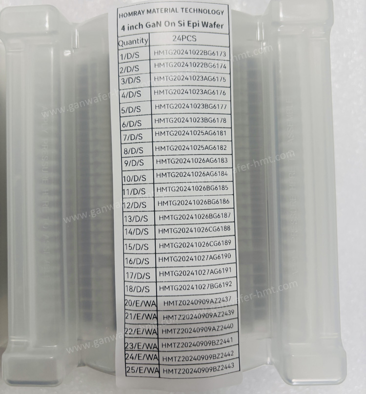
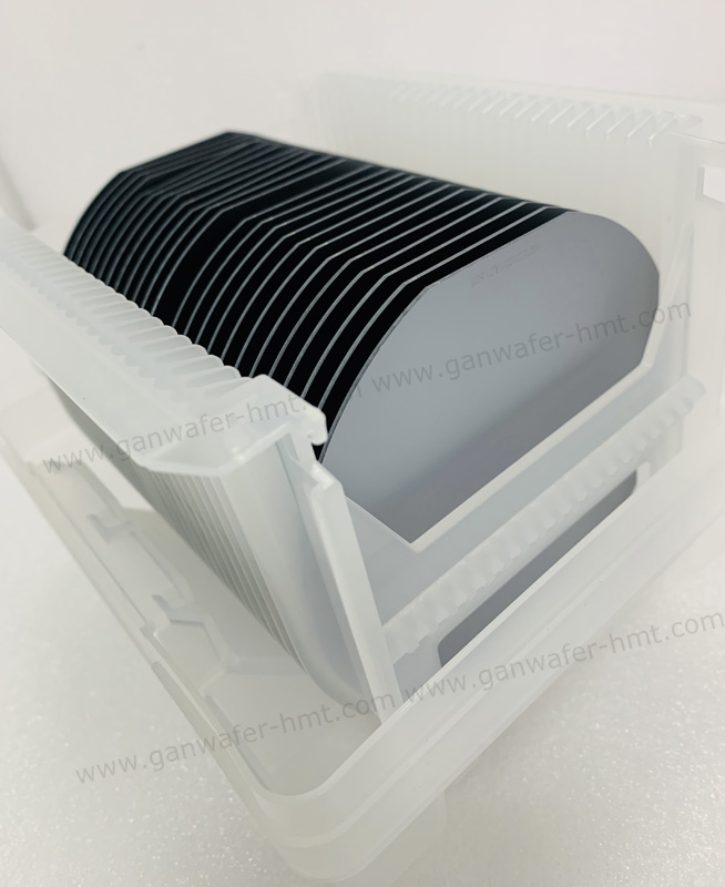
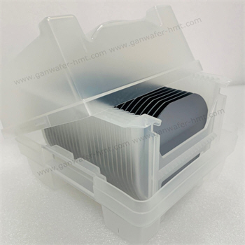
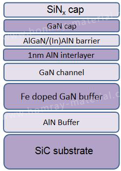
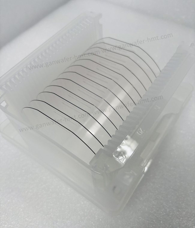
As the leading GaN-on-SiC Epi wafer manufacturer and supplier, HMT produces AlGaN/GaN On SiC HEMT Epi Wafer for RF and power application. We can supply 4 inch and 6 inch u-GaN Cap/Fe Doped GaN Buffer SiC HEMT Epi wafer.The GaN power module has the characteristics of reducing the energy loss during switching and switching, and realizes the high efficiency of energy transmission and utilization.GaN semiconductors are gradually replacing silicon-based products as key components in motors, electric vehicles, smart grids, and renewable energy.
Comparison of first, second and third generation semiconductor materials
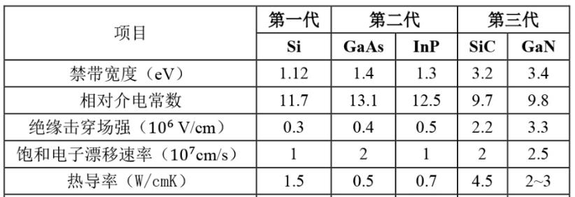
GaN is an extremely stable inorganic compound and also a hard, high-melting material with a melting point of about 1700 ° C, which is mainly synthetic. GaN has a high ionization, band gap of 3.4eV, compared with the second generation of semiconductor compounds has a wider band gap, higher breakdown electric field, higher thermal conductivity and electron saturation rate and better anti-irradiation ability, can be used in high-power, high-speed photoelectric components, is the production of microelectronic devices, optoelectronic devices of new materials.
Structure of GaN-on-SiC Epi Wafer
Related Products
