


SiN Cap GaN-On-Si Epi Wafers Supplier
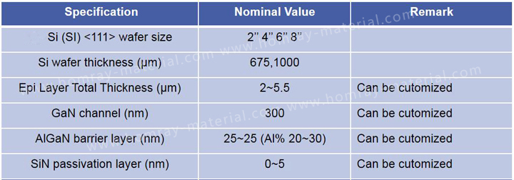
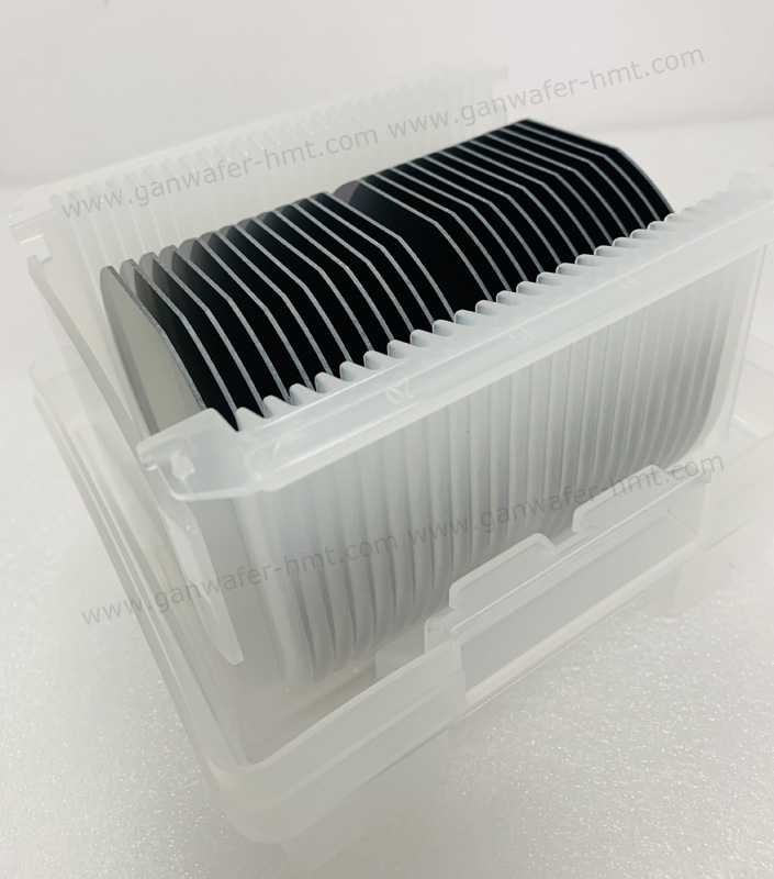
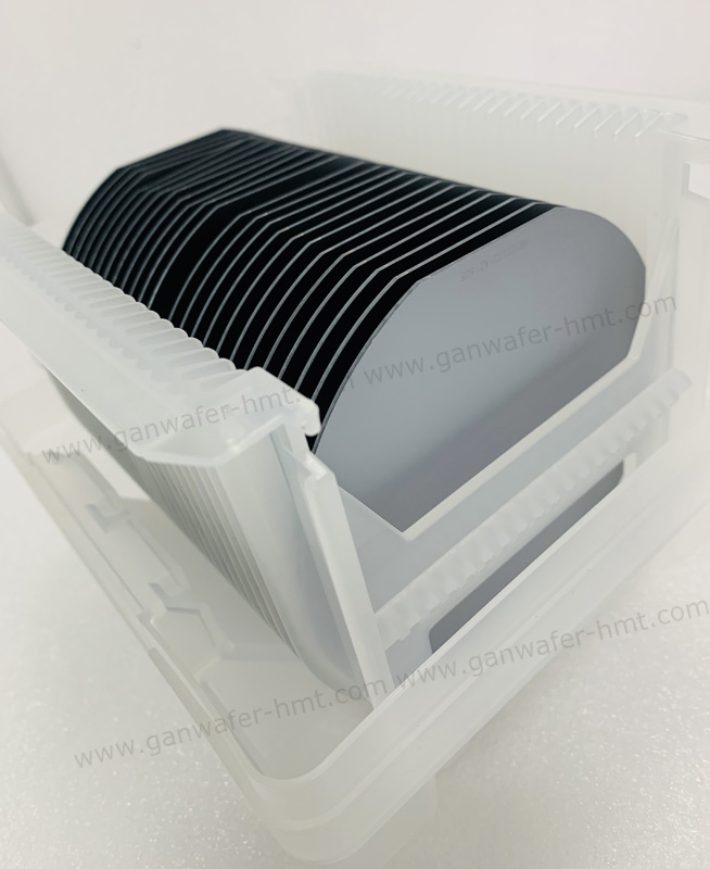
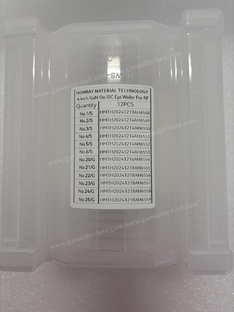
Spec: 4 inch,6 inch,8 inch
Substrate: Silicon
Thickness: 675um 1000um
Cap Layer: GaN or SiN
Product Description
HMT's D-Mode GaN-On-Si Epitaxial Wafers are designed to meet the rigorous demands of next-generation power electronics and RF systems. We supply 4inch to 8inch both SiN cap and GaN cap layer GaN on Si Epi wafers. Leveraging advanced epitaxial growth techniques, this wafer structure ensures optimal performance in high-voltage, high-frequency environments.
Key Structural Parameters & Benefits:
-
SiN or GaN Cap Layer : Enhances surface passivation, reducing leakage currents and improving device reliability.
-
AlGaN Barrier Layer : Facilitates high 2DEG (two-dimensional electron gas) density for superior electron mobility and low on-resistance.
-
GaN Channel : Supports high-power operations with minimal lattice defects.
-
AlGaN Buffer Layer : Minimizes lattice mismatch between GaN and the Si substrate, ensuring crystal integrity.
Si Substrate: We can offer 675um and 1000um thickness Si substrates.
 Applications:
-
High Electron Mobility Transistors (HEMTs)
-
RF amplifiers and 5G communication systems
-
Power converters and inverters
-
Automotive and industrial power modules
Why Choose Our Wafers?
-
High Yield & Consistency: Precise layer control ensures repeatable performance across batches.
-
Thermal Efficiency: Si substrate and optimized layers enable efficient heat dissipation.
-
Scalability: Compatible with standard CMOS fabrication processes for seamless integration.
Optimize your semiconductor designs with our GaN-On-Si D-Mode Epi Wafers—crafted for innovation and durability. Contact us today to request samples or technical specifications.
Related Products


![]() E-mail: kim@homray-material.com tina@homray-material.com
E-mail: kim@homray-material.com tina@homray-material.com
HMT Silicon Carbide (SiC) Substrate Website: www.sicsubstrate-hmt.com