
Power GaN HEMT Epi Wafer On Si Manufacturers
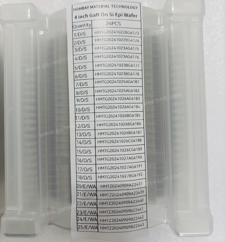
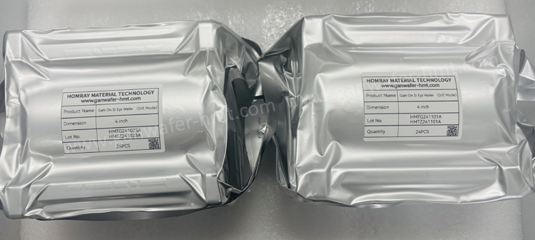
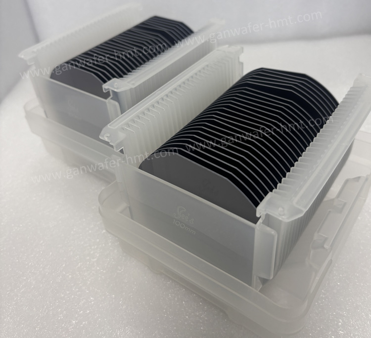
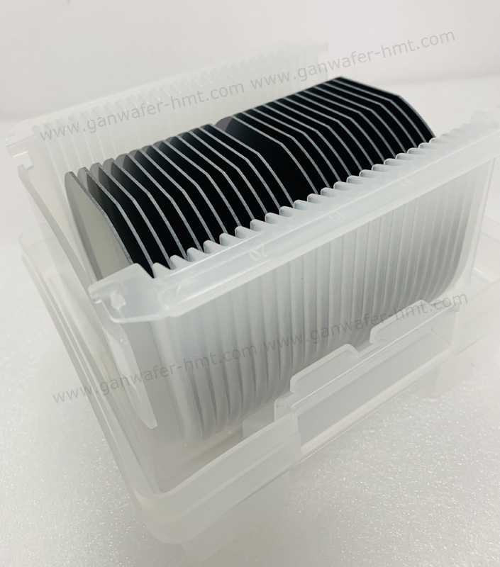
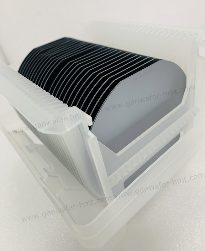
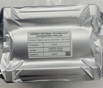
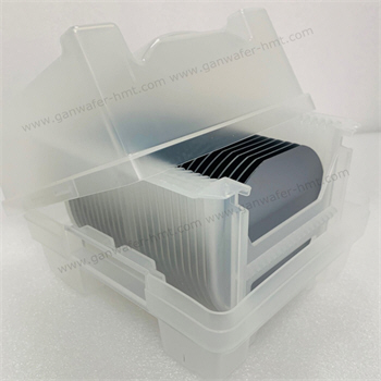
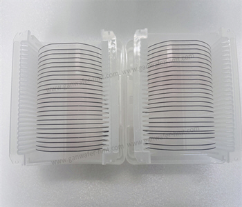
Spec: 4 inch,6 inch,8 inch
Substrate: Silicon
Thickness: 675um 1000um
Cap Layer: GaN or SiN
Product Description
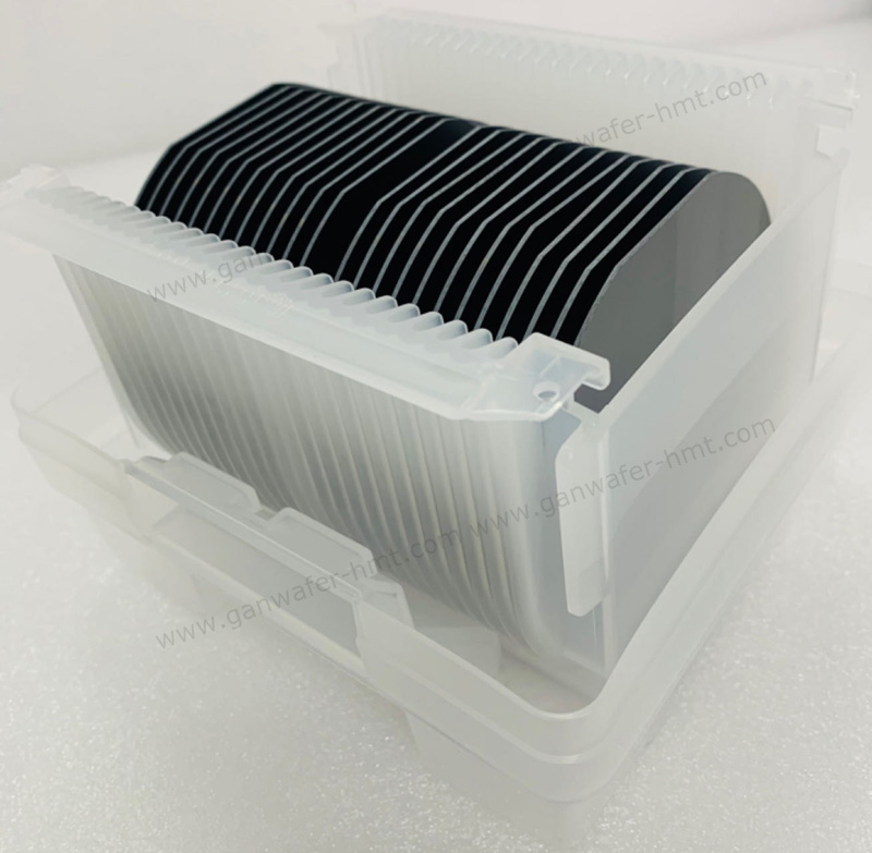
Unlock next-generation power efficiency with our advanced Gallium Nitride (GaN HEMT) Epitaxial Wafers grown on silicon substrates. We always supply 4inch to 8inch GaN on Si Epi Wafers for power HEMT both D-Mode and E-Mode. Designed for high-voltage, high-frequency applications, these wafers combine cutting-edge materials science with scalable manufacturing to deliver unmatched performance in power electronics.
Why Choose Us?
As a leading manufacturer of GaN-on-Si epi wafers, we ensure industry-leading epitaxial layer uniformity, defect control, and customizable doping profiles to meet stringent OEM requirements. Our wafers empower designers to push the limits of power efficiency while reducing system size and cost.
Key Specifications:
-
Wafer Sizes: Normal 6-inch and 8-inch options for seamless integration with existing Si-based fabrication lines. Even 2inch and 4inch,we can also produces.
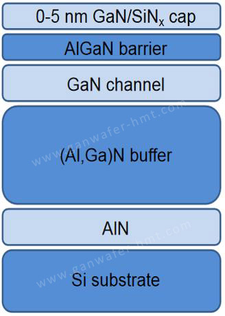
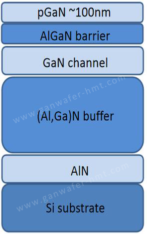
Structure: AlGaN/GaN heterostructure on Si, engineered for optimal 2DEG (Two-Dimensional Electron Gas) density and carrier mobility.
-
Breakdown Voltage: Up to 650V+, enabling robust operation in high-power environments.
-
Thermal Management: Low thermal resistance thanks to optimized Si substrate compatibility.
Applications:
-
Electric Vehicle (EV) powertrains and fast-charging infrastructure
-
5G base stations and telecom power supplies
-
Industrial motor drives and renewable energy systems
-
Consumer fast-charging adapters and UPS systems
Related Products


![]() E-mail: kim@homray-material.com tina@homray-material.com
E-mail: kim@homray-material.com tina@homray-material.com
HMT Silicon Carbide (SiC) Substrate Website: www.sicsubstrate-hmt.com