
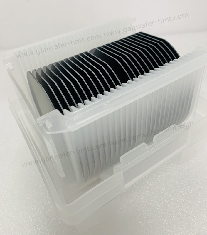
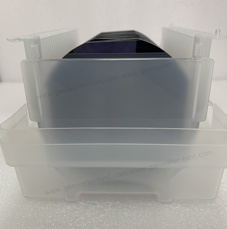
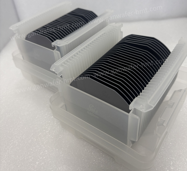
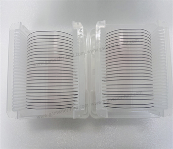
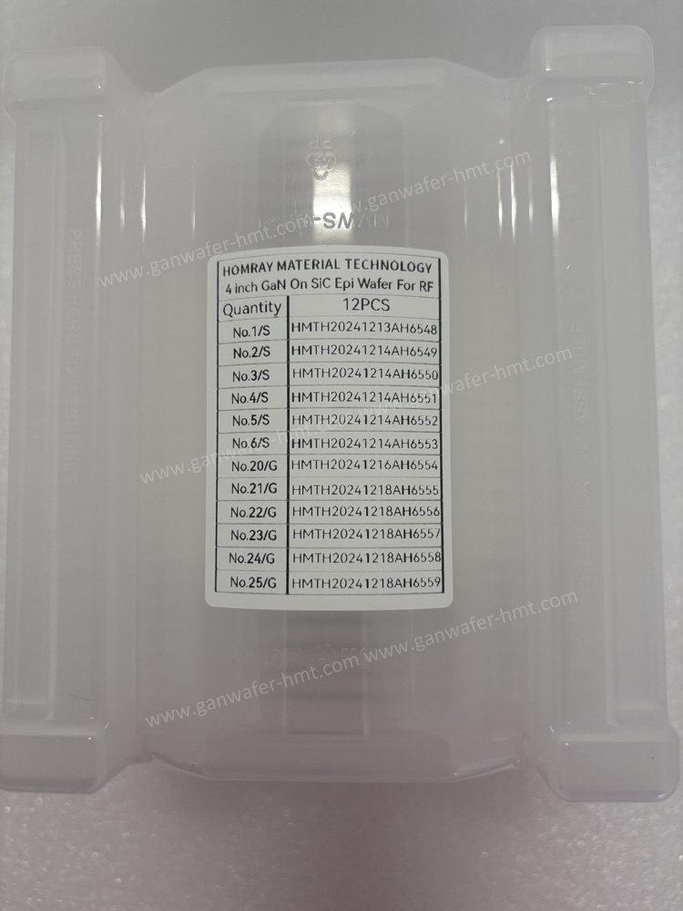
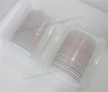
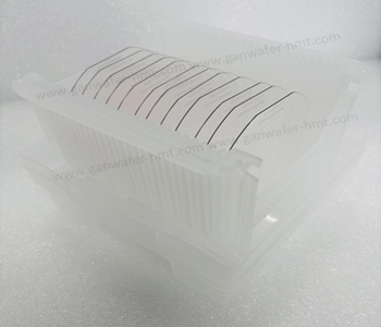
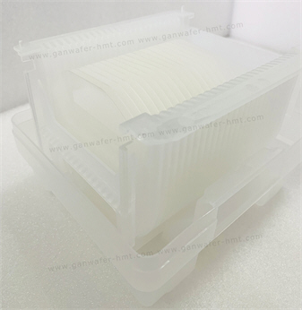
GaN/SiN Cap AlGaN Barrier Epi with 25% Al HEMT
Spec: 4 inch,6 inch,8 inch
Substrate: Silicon
Thickness: 675um 1000um
Substrate grade: Production
Product Description
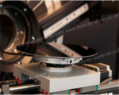
HMT focus on 4 inch to 8 inch GaN/SiN Cap AlGaN Barrier Epi with 25% Al HEMT manufacturing. we manufacture D-mode,E-mode and RF structure of GaN on Si epi wafer. Due to the high melting point of gallium nitride (GaN) and the high saturated vapor pressure, it cannot exist in the form of single crystals in nature, and it is very difficult to prepare the film by the general bulk single crystal growth method, and it must be prepared by the epitaxy method. HMT use MOCVD method for the preparation of GaN epi.
Application of GaN Epi Wafer
1. GaN devices are widely used in wireless devices, power amplifiers with frequencies up to 100 GHz, mainly for military radar, satellite transmitters, and general-purpose RF amplification. Because GaN devices are used for high voltage (up to 1,000 V), high temperature, and fast switching, they are also incorporated into a variety of switching power applications such as DC-DC converters, inverters, and battery chargers.
2. GaN material series has low heat generation rate and high breakdown electric field, and is an important material for the development of high temperature and high power electronic devices and high frequency microwave devices. At present, with the progress of MBE technology in GaN material application and the breakthrough of key film growth technology, a variety of GaN heterostructures have been successfully grown. New devices such as metal field effect transistor (MESFET), heterojunction field effect transistor (HFET) and modulated doping field effect transistor (MODFET) have been prepared by using GaN materials.
GaN On Silicon HEMT Epitaxy wafer

Related Products


![]() E-mail: kim@homray-material.com tina@homray-material.com
E-mail: kim@homray-material.com tina@homray-material.com
HMT Silicon Carbide (SiC) Substrate Website: www.sicsubstrate-hmt.com