
6 inch pGaN-on-Si Epi Wafer Supplier
GaN-On-Si Epi Wafer For Power HEMT-E Mode
Substrate Diameter: 4-8 inch Silicon
Substrate Thickness: 675,1000um
Cap Layer: pGaN
Product Description
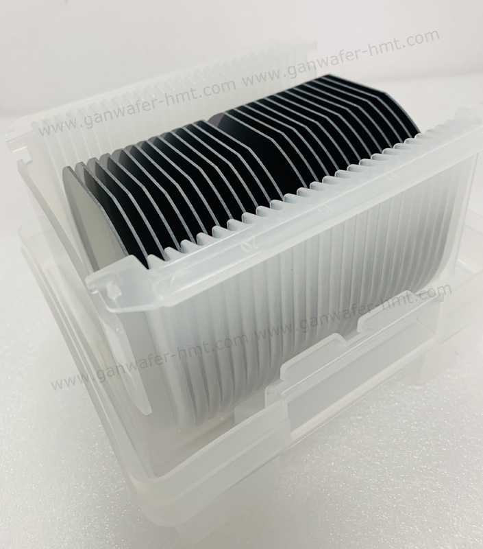
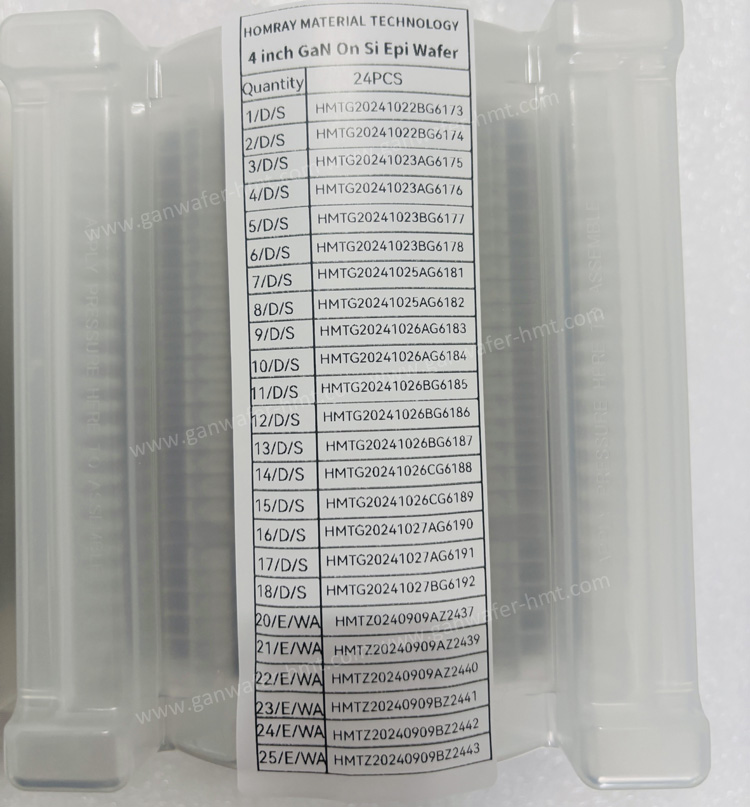
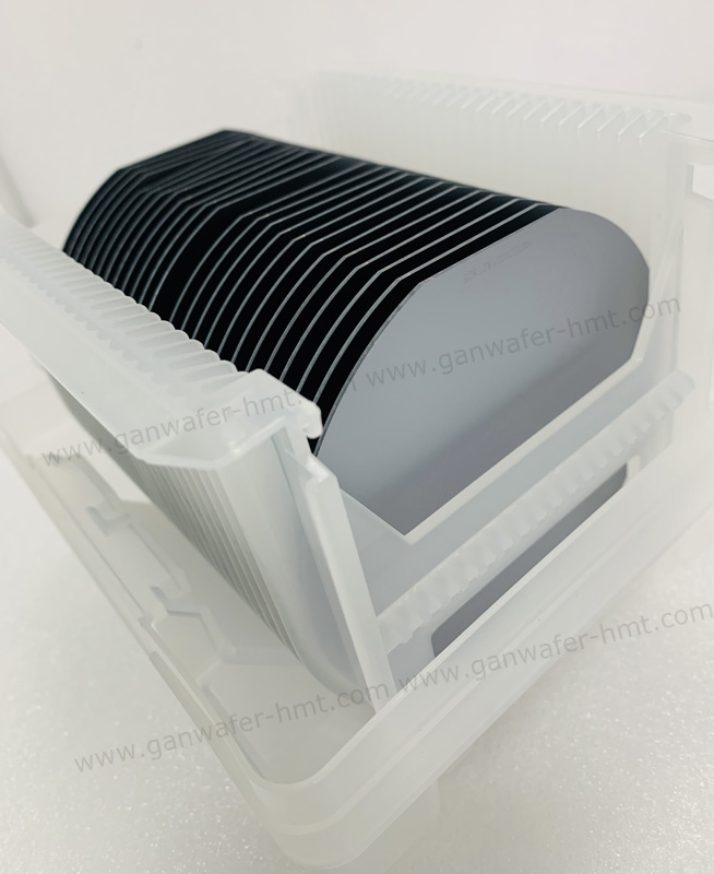
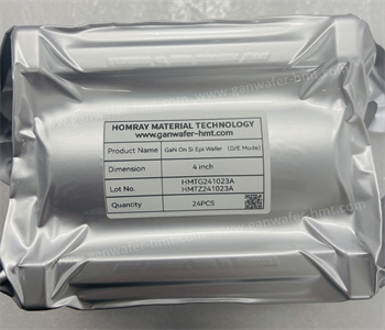
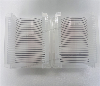
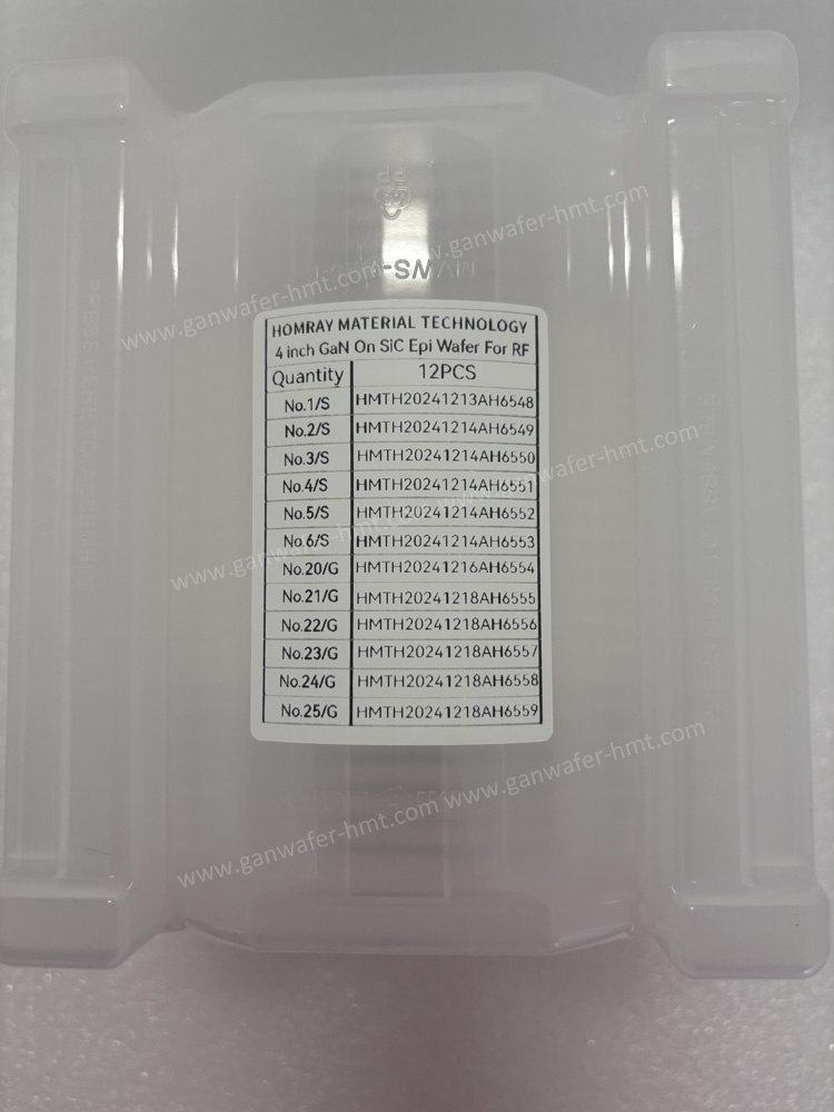
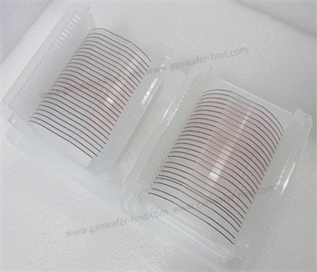
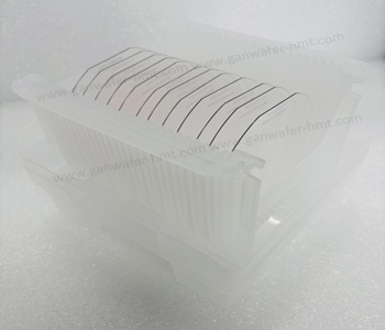
As the professional GaN Epi wafer supplier, we produce 4 inch 6 inch and 8 inch pGaN/AlGaN-on Si Epi Wafers by MOCVD. pGaN Cap Layer doping with Mg and thickness 90-100nm. Our normal pGaN on Si Epi Wafer structure as below:
pGaN Cap Layer
AlGaN Barrier
GaN Channel
(Al,Ga)N Buffer Layer
AlN Nucleation Layer
675µm or 1000um Si Substrate

GaN Epitaxy Wafers Applications:
-
High-Electron-Mobility Transistors (HEMTs) for RF and microwave systems
-
High-efficiency DC/AC power converters and inverters
-
Automotive electric vehicle (EV) powertrains and charging infrastructure
-
5G base stations and millimeter-wave communication devices
Key Differentiators:
-
Defect-Reduced Growth: Advanced epitaxial techniques ensure minimal dislocations for higher device yield.
-
Thermal Optimization: AlN layer and Si substrate synergize to dissipate heat efficiently, even under extreme loads.
-
Scalable Production: Compatible with standard semiconductor manufacturing workflows, enabling rapid prototyping and mass production.
Elevate your power electronics designs with our pGaN Epitaxial Wafers—crafted to meet the rigorous demands of modern technology. Request a datasheet or sample today to experience industry-leading quality.
Related Products


![]() E-mail: kim@homray-material.com tina@homray-material.com
E-mail: kim@homray-material.com tina@homray-material.com
HMT Silicon Carbide (SiC) Substrate Website: www.sicsubstrate-hmt.com